App note: 4-20mA current loop primer

Basics of current loop App note from Murata, discussing the basic theory of the 4-20mA current loop operation. Link here (PDF)

The 4-20mA current loop is a common method of transmitting sensor information in many industrial process-monitoring applications. A sensor is a device used to measure physical parameters such as temperature, pressure, speed, liquid flow rates, etc. Transmitting sensor information via a current loop is particularly useful when the information has to be sent to a remote location over long distances (1000 feet, or more). The loop’s operation is straightforward: a sensor’s output voltage is first converted to a proportional current, with 4mA normally representing the sensor’s zero-level output, and 20mA representing the sensor’s full-scale output. Then, a receiver at the remote end converts the 4-20mA current back into a voltage which in turn can be further processed by a computer or display module.

App note: Conductive plastic technology

App note about conductive plastic used on motion transducers from Vishay. Link here (PDF)

The polymer film track has a conductive plastic paste laid upon it. This paste includes an inert filler of carbon black which constitutes the basis of Vishay SFERNICE’s technology for manufacturing precision potentiometers.
The resistive track obtained can be used:
• inside a cylindrical housing for making a rotational potentiometer
• on a flat support when manufacturing a linear motion transducer.
This method of producing the plastic film creates a resistive track which is exceptionally uniform in its resistivity and which allows excellent results regarding linearity.

App note: Optimizing output power of power op amps

Enhancing the performance of power op amps discussed in this app note from Apex Microtechnology. Link here (PDF)

Power op amps are attractive because they reduce circuit design time enormously. Assembly costs of the power op amp design amount to a fraction of the discrete counterpart due to vastly reduced parts count. Careful attention to the power aspects of a circuit is required, as the well known op amp design rules based on low power devices. The objectives are to maximize reliability plus optimize output power and system efficiency. This application note points out some optimizing techniques and some areas to be especially watchful.

App note: Migrating from FT2232D to FT2232H

App note on FTDI’s FT2232 USB bridge migration, with full detailed list of capabilities on the newer FT2232H. PDF link can be found here

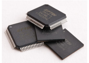
This Application Note details the differences between the FT2232D and FT2232H to help customers design with FT2232H as this newer, high speed USB device has better performance.

App note: Continuous DC current ratings of International Rectifier’s large semiconductor packages

App note from International Rectifier on how to optimize the maximum current handling of power FETs. Link here (PDF)

There is a trend within the discrete power component industry of late to increase the dc current rating for low on-resistance devices to levels that historically have not been seen. This trend has accelerated as power transistor manufacturers introduce higher current / lower voltage designs. Mature JEDEC package designs, originally intended decades ago for dc currents on the order of 10’s of Amperes are now emerging as capable of 100’s of Amps. Is this due to some significant improvement in package materials / design or is this all smoke and mirrors? The answer is a little of both.

App note: AC film capacitors in connection with the mains (≤ 60 Hz)

Suppressing EMI from mains and getting power in-series with a capacitor are just the two main function of these front line capacitors and is discussed in this app note from Vishay. Link here (PDF)

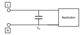
Because of the high energy availability and the severe environment of surge voltages and pulses, applications of capacitors in connection with the mains must be chosen carefully.
Two kinds of connections, and thus two kinds of applications, can be distinguished.
One is where the capacitor is directly connected in parallel with the mains without any other impedance or circuit protection, and another where the capacitor is connected to the mains in series with other circuitry.

App note: ESD protection for super speed USB 3.0 ports

Design guide app note from Alpha & Omega Semiconductor on USB 3.0 protection. Link here (PDF)

USB 3.0 is an enhanced version of the USB 2.0, with up to 5Gbps data rate. USB 3.0 has 10 times the performance over USB 2.0. Legacy device continue to work when plugged into new host connector albeit at USB 2.0 speeds. USB 3.0 maintains this backward compatibility by adding an addition pairs of SuperSpeed differential data lines, SSRX+/- and SSTX+/- with the existing pair of USB 2.0 data line, D+ and D-. The SSRX and SSTX is the differential data line that we are focus in the PCB layout and ESD protection.
A carefully designed PCB layout in combination with rugged ESD protection is vital for a robust operating system.

App note: Direct current ammeters

App note from Murata about digital ammeter and things to consider implementing them. Link here (PDF)

There is a trend to replace older, analog-style readouts with modern digital displays. As one might expect, the conversion is not always a trivial task. This is especially true when the conversion involves older, moving-vane (“pointer” style) analog ammeters. The typical analog ammeter has only two wires to contend with, and the required shunt resistor is sometimes built-in to the meter itself. By comparison, its digital replacement may have as many as fi ve or six input terminals. The project gets even more complicated when you include the required external current shunt. Hopefully, after reading this application note, you will have the necessary information to avoid the most common pitfalls associated with digital ammeter installations.

App note: Some thoughts on DC/DC converters

Basis App note of modern DC/DC converters from Analog Devices. Link here (PDF)

Many systems require that the primary source of DC power be converted to other voltages. Battery driven circuitry is an obvious candidate. The 6V or 12V cell in a laptop computer must be converted to different potentials needed for memory, disc drives, display and operating logic. In theory, AC line powered systems should not need DC/DC converters because the implied power transformer can be equipped with multiple secondaries. In practice, economics, noise requirements, supply bus distribution problems and other constraints often make DC/DC conversion preferable. A common example is logic dominated, 5V powered systems utilizing ±15V driven analog components.
The range of applications for DC/DC converters is large, with many variations. Interest in converters is commensurately quite high. Increased use of single supply powered systems, stiffening performance requirements and battery operation have increased converter usage.

App note: The Alexander Current-Feedback audio power amplifier

An old App note for audio enthusiast from Analog Devices about Current-Feedback approach in audio power amps its designs and history by Mark Alexander. Link here (PDF)

The subject of power amplifier design is one of those controversial areas of audio engineering that continues to receive intense debate, despite the fact that there are literally dozens of papers available to guide the designer. Many different topologies have evolved from the relatively modest beginnings of solid state power amplifier design in the late 1950s and early 1960s, and this has lead to a few very unique and original designs. A substantial number of transistorized amplifiers that were built during these early years were little more than redesigns of vacuum tube circuits with lower voltage supply rails, and often had performance levels that left a great deal to be desired. Quite a few of them sounded significantly worse than their thermionic predecessors. The “real revolution” in audio power amplifier design actually occured during the 1970s and introduced such new innovations as direct coupling, fully complementary design, pseudo Class A biasing, and current dumping.

App note: Understanding dual terminator resistor networks

App note from Vishay about the dual terminator resistor network and how to check its internal resistor values. Link here (PDF)

One of the least understood resistor network schematics in the industry today is the dual-resistor terminator schematic shown in the 8-pin SIP and in the 16-pin DIP configuration.
This schematic shows up in both commercial / industrial parts and in military parts. Commercial parts are sometimes identified as TTL dual-line terminators or as pulse-squaring terminators.

App note: Phase noise measurement guide for oscillators

App note from SiTime about phase noise, its fundamental and going to actual measurements. Link here

Phase noise is one of the fundamental metrics for oscillators. An experienced engineer can tell a lot about the quality of an oscillator and whether it fits the application by looking at the phase noise plot. RF engineers focus on the phase noise levels at certain carrier offset frequencies to make sure that the required modulation scheme can be supported. Professionals designing high speed serial links like 40GbE will apply a band pass filter to phase noise of a reference clock, integrate it, and convert it to phase jitter to predict the bit error rate of a system.

App note: Transmission-line effects influence high-speed CMOS

Old app note from ONSEMI but still a good reference when designing with high speed CMOS devices. Link here (PDF)

Unlike low-power, metal-gate CMOS, high-speed 54HC/74HC devices readily drive long cable runs and backplanes. While the family maintains CMOS’s traditional noise immunity, you must watch transmission-line effects in such applications.

App note: Reading onsemi IGBT datasheets

Helpful app note from ONSEMI that will guide you to their IGBT parameters. Link here (PDF)

The Insulated Gate Bipolar Transistor is a power switch well suited for high power applications such as motor control, UPS and solar inverters, and induction heating. If the application requirements are well understood, the correct IGBT can easily be selected from the electrical properties provided in the manufacturers’ datasheet.

App note: High-side smartFETs with analog current sense

App note from ONSEMI about their high side SmartFETs and their specific application. Link here (PDF)

The “end requirement” from a high side SmartFET is to switch loads, and there are different alternatives, available in market, towards that end. Relays, for instance, have been used for long in the industry to switch various automotive loads, especially those requiring high current activation. With a continual reduction in the weight and size of automotive components and assemblies, there has been an evident transition from relays to semiconductor switches that take up less area and also offer improved noise immunity and lower electromagnetic interference as compared to relays.

App note: SEPIC converter analysis and design

Wide input voltage is a specialty of this type of DC-DC converter, here’s an app note from ON Semiconductors on SEPIC converters. Link here (PDF)

The single−ended primary−inductor converter (SEPIC) is a type of DC/DC converter that allows the electrical potential (voltage) at its output to be greater than, less than, or equal to that at its input.
Like other DC−DC switch−mode power supply converters, the SEPIC exchanges energy between inductors and capacitors to convert from one voltage to another voltage. Typical applications for a SEPIC regulator are:
• Battery−operated equipment and handheld devices
• NiMH chargers
• LED lighting applications
• DC power supplies having a wide range of input voltages

App note: Method of suppressing increase in surface temperature of shunt resistors

App note from ROHM Semiconductor about their shunt resistor mounting designs to keep heat away. Link here (PDF)

Shunt resistors are widely used for current sensing in automotive and industrial applications. In the automotive sector, as vehicles become more complex and the number of motors and ECUs grows, applications need to be configured in a limited space.
As a result, components are being mounted more intensively and customers require shunt resistors – one of the components mounted on vehicles – that are more power efficient and compact. Accordingly, the thermal design of products and circuit boards has become an important issue.

App note: Effect of PCB design on temperature coefficient of resistance

App note from ROHM Semiconductor on the importance of sense trace/line arrangement on PCB designs. Link here (PDF)

While resistance, power rating and size are important considerations when using shunt resistors, tolerances that affect the accuracy of the detected voltage must also be considered. These tolerances include the temperature coefficient of resistance and the tolerance of resistance at room temperature.
The temperature coefficient of resistance indicates the change in resistance value due to a change in temperature of the resistor. Since resistance is affected by component temperature rise as current flows through and power is consumed, and ambient temperature changes, the temperature coefficient of resistance is an important factor in accurately detecting current values.

App note: Types of capacitors used for output smoothing of switching regulators and their precautions

Another app note from ROHM Semiconductor on various capacitors used for output smoothing. Link here (PDF)

In recent years, it has become a common practice to recommend multilayer ceramic capacitors for the output smoothing of switching regulators due to the stability of their temperature characteristics and the reduction on the mounting area. On the other hand, they are increasingly being replaced by low-cost, high-capacity aluminum electrolytic capacitors and conductive polymer hybrid aluminum electrolytic capacitors.