App note: Optical isolator for I2C Bus System

App note from Vishay on galvanically isolating I2C bus by optocoupler. Link here (PDF)

The I2C bus, also known as inter-IC bus, is a bidirectional, two-wire, multi-user bus. It was developed by Philips Semiconductors to connect microcontrollers, EEPROMs, A/D and D/A converters, I/O interfaces, and other peripherals.
For optical isolation between master and slave, an optocoupler is the perfect solution. Due to galvanic isolation, an optocoupler helps to break up ground loops and reduces the electrical noise due to optical light transmission across an isolation barrier.
It can restore the logic level and can be used for signal level transforming between different voltage level domains, e.g. from 5 V to 3.3 V or 24 V.
One channel is required for the serial clock line (SCL) and two channels for the serial data line (SDA) to transmit the data from master to slave and back.

App note: Optocoupler as optical isolator for RS-232 Bus System

Using optocoupler for galvanic isolation of RS-232 Bus introduced in this app note from Vishay. Link here (PDF)

The RS-232 bus is a serial, single-ended bus system with a data transfer rate up to 115.2 kBd. The application areas are computer to computer or computer to peripheral devices communication, like a printer, mouse, and so on.
In case of electrical noise, coupling effects, or level shifting requirements, an optocoupler is a perfect solution for isolating two devices. Due to galvanic isolation, an optocoupler helps to break up ground loops and reduce the electrical noise due to optical light transmission across an isolation barrier. It can also restore the signal logic level and further be used for signal level transforming between different voltage domains, e.g. from 5 V to 3.3 V.

App note: NVT4557/NVT4558/NVT4858 voltage-level translator layout guideline

App note from NXP Semiconductors on proper board layout guideline for NVT4557/NVT4558/NVT4858 voltage-level translators for optimal operation. Link here (PDF)

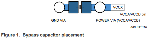
High performance digital signals on modern microprocessors are designed using advanced CMOS process to take advantage of its low power consumption. However, CMOS logic has very fast edge rates in the range of 1 ns to 2 ns. PCB traces might exhibit ringing, signal degradation and reflection due to the effect of the signal’s fast rise and fall time contributed by the PCB transmission characteristic.
The NVT4858 is an SD 3.0 compliant dual voltage level translator with auto-direction control. The NVT4557/4558 is a SIM SIO-7816 Smart Card compliant dual voltage level translator with auto-direction control.

App note: Simple guide to improving ripple rejection ratio of LDO regulators

App note from Toshiba on improving LDO regulators PSRR. Link here (PDF)

This document explains the principles of suppressing ripple of the output voltage, which is caused by the ripple of the input , i.e. the ripple compressibility (PSRR). It also explains the frequency characteristics of PSRR and the effects of the output capacitor.

App note: Tips for selecting level shifters/voltage translation ICs

Reference app note from Toshiba about voltage translator selection. Link here (PDF)

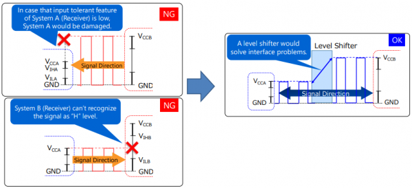
This application note discusses how to select the right level shifter (also known as voltage translation IC).
In some cases, CMOS logic ICs with a TTL-level input or an open-drain output provide levelshifting without using costly level shifters. It is therefore important to select the optimum device, taking available board space and part costs into consideration.

App note: ESD protection audio input and output lines

Audio port protection discussed in this app note from Littlefuse. Link here (PDF)

Externally generated ESD pulses are introduced through the Audio jacks (headphone, microphone, RCA-type plugs, etc.) and travel through the connector onto the system board. Once on the board, they will propagate down the signal lines toward the integrated circuits(IC). Most ICs are designed with 2,000V of internal ESD protection. It is not uncommon to measure ESD transients in consumer environments over 8,000V.Without sufficient protection, the Audio system can experience visual distortion or corrupted data. In addition, the IC could be permanently damaged rendering the whole system inoperable.

App note: Coordinated circuit protection options for LED lighting

App note from Littelfuse on protecting LED lights from overloaded circuits, overvoltage and electrical shorts assuring safety on customers from these hazards. Link here (PDF)

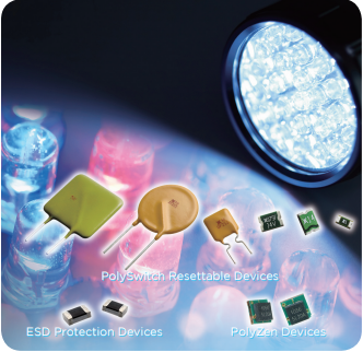
LED technology has advanced rapidly, with improved chip designs and materials facilitating development of brighter and longer-lasting light sources that can be used in a wide spectrum of applications. A growing awareness of the need to reduce energy costs has also made LED lighting increasingly popular.
In spite of the growing popularity of the technology, LED light manufacturers continue to wrestle with the fact that LED luminaires are very heat sensitive. Excessive heat or inappropriate applications can dramatically affect performance.

App note: Single channel smart load switch use and selection

App note from Diodes Incorporated present you their solution to put a safeguard on your load from transients spikes and shorts, these load switch also do have monitoring pins in order to show the condition of the supply line. Link here (PDF)

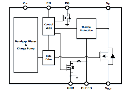
Single Channel Smart load switch provides a component and area-reducing solution for efficient power domain switching. In addition to integrated control functionality with ultra-low on resistance (<15 mΩ), this device offers system safeguards and monitoring via the fault protection (Short circuit protection, SCP) and power good signal. This cost effective solution is ideal for power management and hot-swap applications requiring low power consumption in a small footprint.

App note: Suppression of transients in an automotive environment

App note from Littelfuse about automotive electrical noises and where they came from and what to do with them in order to prevent it from going to your circuit. Link here (PDF)

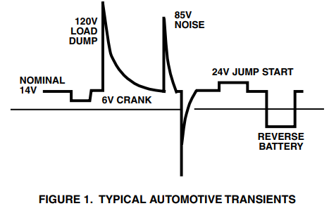
As the control circuitry in the automobile continues to develop, there is a greater need to consider the capability of new technology in terms of survivability to the commonly encountered transients in the automotive environment. The circuit designer must ensure reliable circuit operation in this severe transient environment. The transients on the automobile power supply range form the severe, high energy, transients generated by the alternator/regulator system to the low-level “noise” generated by the ignition system and various accessories.

App note: An introduction to transient voltage suppression devices

App note from Littelfuse introduces you to their TVS options specifically fit to your circuit protection needs. Link here (PDF)

Transient Voltage Suppression (TVS) protection devices such as shielded cables, crowbars, filters and clamping devices have been widely used for a number of years to solve EMI problems. These TVS devices can be used to achieve higher EMI higher immunity levels without significantly adding to the cost and complexity of the circuit. The attributes of traditional TVS devices will be compared to the features of a relatively new option, the avalanche diode TVS EMI filter. Recent advancements in IC manufacturing technology provide the TVS diode with several technical and cost advantages compared to traditional EMI devices.

App note: Buck-Boost charger MOSFETs

Selecting the desired MOSFET fit for Buck-Boost for higher efficiency in power supply and battery charging section discussed in this app note from Alpha & Omega Semiconductors. Link here (PDF)

The wide adoption of USB Type-C PD makes the notebook PC charger move to four MOSFET buck-boost charger topology to allow for wide range input voltage (5-20V). After a suitable controller is selected, the specified Power MOSFETs in buck-boost charger are essential for achieving higher efficiency and high-power density design.
In this application note, we will only discuss the USB power delivery specification for an adapter supplying 5A/100W and expect the reader to understand the basic operation of buck-boost topology. It is critical to select suitable MOSFETs regarding efficiency, thermal, and space limitation, to meet the system-level requirements. 30V MOSFETs can be used for input voltage below 20V.
Based on given wide input voltages, output voltages, and current, the designer must understand the tradeoff among the different loss mechanisms in the MOSFET. These MOSFET losses include: switching loss, conduction loss, and reverse recovery loss. Losses are minimized by selecting the best MOSFETs from its electrical characteristics.

App note: Design considerations on Solid-State Relays in DC configuration

Solid-state relays uses app note by Vishay in DC application with resistive, capacitive and inductive loads. Link here (PDF)

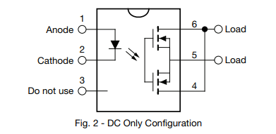
A solid-state relay (SSR) is an electronic switching device in semiconductor technology. An SSR has a high efficient GaAlAs infrared emitter on the input which is optically coupled to the high performance MOSFETs at the output.
An SSR is capable of switching AC loads where both output MOSFETs are required as well as DC loads where one MOSFET, or two in parallel, can be used.

App note: TJA1101B automotive Ethernet PHY

App note from NXP introducing their network solution TJA1101B to handle Ethernet in automotive environment. Link here (PDF)

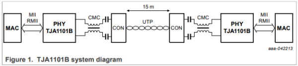
The TJA1101B is a 100BASE-T1 compliant Ethernet PHY optimized for automotive use cases. The device provides 100 Mbit/s transmit and receive capability over a single unshielded twisted pair cable, supporting a cable length of at least 15 m. Optimized for automotive use cases like IP camera links, driver assistance systems and back-bone networks, the TJA1101B has been designed for automotive robustness and ISO 26262 ASIL-A compliance, while minimizing power consumption and system costs.

App note: How to calculate power losses in Gen 5 diodes

App note from Vishay which focuses on the diode’s losses present during the forward and reverse condition. Link here (PDF)

In the forward condition, diodes carry the current while showing the lowest resistance at the current flow (ON state) and the lowest possible voltage anode to cathode. In the reverse condition, the voltage anode to cathode across the diode is negative (OFF state) and the device is like an open circuit; the current flowing through the diode the leakage current is very small.
The transition between the forward and reverse conditions is called recovery. Forward recovery is when a diode goes from the OFF state to the ON state. Reverse recovery is when a diode goes from the ON state to the OFF state. These transitions are associated with losses, known as switching losses. Usually, forward recovery losses are negligible; but reverse recovery losses particularly those in high frequency circuits can be a non-negligible portion of losses present in the diode.

App note: Extending op amp operating range via bootstrapping

App note from Analog Devices discussing bootstrapping its rail voltage to compensate operating range of an op amp. Link here (PDF)

When an off the shelf operational amplifier (op amp) cannot provide the signal swing range needed for a particular application, the engineer is faced with using a high voltage op amp or designing a discrete solution—both choices being potentially costly avenues to solving the problem. A third option, bootstrapping, can be an inexpensive alternative to these approaches for many applications. A bootstrapped power supply circuit involves a fairly straight-forward design exercise in all but the most dynamic performance demanding applications.

App note: The effect of long-term drift on voltage references

App note from Analog Devices on ways to eliminate drifts on voltage refs. Link here (PDF)

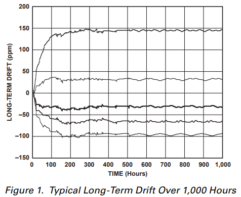
Long-Term Drift (LTD) in voltage references is a parameter that can be confusing and misleading. It is given as a typical parameter in data sheets, but can cause significant accuracy limitations in system. Unlike tempco and initial accuracy, where a one-time calibration can be used to eliminate these errors, attempts to reduce LTD requires frequent system calibration. This can be both time consuming and expensive. Therefore, it is important to understand the significance of LTD.

App note: Small, simple, PWM buck controller can replace high current LDOs

Compact buck converter design from ONSEMI an alternate solution for LDOs producing larger current. Link here (PDF)

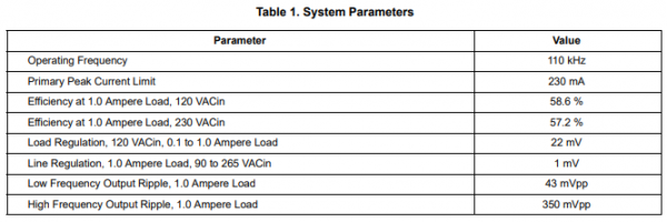
Low dropout, linear regulators, or LDOs, are typically used for post−regulation because they are easily implemented and provide a relatively noise−free power source. However, for higher currents, such as 1.0 A and above, LDOs take up a great deal of space and can dissipate too much power and thus heat. For low dropout applications where you need another voltage rail, and you already have a 5.0 V or 3.3 V rail, a simple PWM buck converter provides a more efficient choice than a linear regulator.

App note: Isolated precision regulation of a single 1.8 Volt output from a universal line input

Isolated precision SMPS design from ONSEMI. Link here (PDF)

The following Application Note describes an off–line switching power supply utilizing a precision programmable reference to regulate a 1.8 volt output. The center of the app note is the MC33363B, a monolithic SMPS controller with a 700 volt power switch, and the NCP100, a sub–one volt precision programmable reference.

App note: USB power delivery changes the game

Great read on this white paper from Renesas about the history of USB power delivery. Link here (PDF)

Connections between equipment for data transfer and power are being revolutionized by the adoption of ‘USB Power Delivery’, a version of USB that allows up to 100W to be passed in either direction. This white paper traces the history of the standard and its capabilities up to the present day with USB Type-C TM cables and connectors enabling ‘Superspeed’ communication while providing bi-directional power transfer for peripheral operation and battery charging. Practical advantages of USB Power Delivery are described along with the wider benefits of reduction in complexity and number of interconnections and their environmental impact. Integrated circuit solutions for the design of interfaces to control power flow are introduced.