App note: Opto-electrical isolation of the I2C-bus (operating the bus between points with different local ground potential)

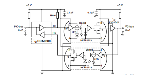
App note from NXP Semiconductors shows I2C-bus galvanic isolation solution by splitting the bi-directional bus to unidirectional logic signals and passing them through opto-isolator couplers. Link here (PDF)

Many systems that can benefit from the advantages of I2C-bus control are not allowed to share any common reference signal (ground) potential. To prevent any chance of electrocution, AC mains control and medical patient monitoring equipment require a safety isolation barrier, to kilovolt levels, between the system components. Regulations require isolation from telephone lines and Standards require isolation from Ethernet wiring, especially when power is also supplied by the Ethernet wiring (PoE). Techniques enabling reliable I2C communication while addressing these different requirements all require first splitting the normally bidirectional SDA/SCL signals into two uni-directional components and then applying conventional techniques to provide the necessary tolerance to difference in local ground potentials, or to provide total galvanic isolation.

App note: Si70xx temperature sensor designer’s guide

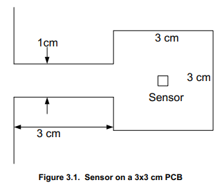
Best way to place/mount temperature sensors to optimize thermal conductivity an App note from Silicon Labs. Link here (PDF)

The Si70xx temperature sensors work by measuring the Vbe of an on chip transistor at two currents in a precise ratio to measure temperature. The resulting voltage is digitized, calibrated and linearized such that after conversion the temperature can be easily calculated.
Thus the temperature being measured is the temperature of the die within the Si70xx package. This die is mounted on a metal lead frame. It is useful to think of the leadframe as the thermal input to the die since the thermal resistance from the paddle to die is quite low (a few °C/W) while the thermal resistance through the top of the package is quite high (over 1000 °C/watt for convective heat transfer).

App note: Smart battery charger by LPC865 with SMBus interface

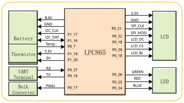
App note from NXP Semiconductors on their Arm Cortex-M0+ based low cost MCU LPC865 smart battery charger. Link here (PDF)

The application of batteries is everywhere: smartphones, notebook computers, wearable devices, handheld electronic products, smart small appliances, and so on. Information about the state of batteries is important for the user, for example, the battery temperature, voltage, current, capacity, how much time is needed to charge the battery and to get it depleted. It is important to ensure the safety of battery charging and provide a smooth and controllable charging curve. The abovementioned requirements are expected to be realized by a smart charger. A smart charging solution implemented with LPC865 is recommended.

App note: Choosing an input resistor for a Microelectronic Relay

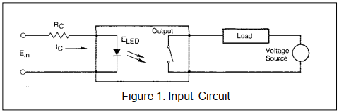
App note from Infineon Technologies about properly choosing resistor value in series to Microelectronic Relay. Link here (PDF)

The International Rectifier Photovoltaic Relay (PVR) devices are current-controlled microelectronic relays with a specified current which must be supplied for turn-on. Therefore, a current limit resistor is necessary when operating from a voltage source. This application note gives the procedure for determining the proper resistor to program the microelectronic relays to operate from any control voltage.

App note: Introduction to Power PROFET

App note from Infineon Technologies introducing their automotive high side switches PowerPROFET. Link here (PDF)

Smart, high-side power switches from Infineon® are designed to control all types of resistive, inductive, and capacitive loads. These devices provide protection and diagnostic functions and are specially designed to drive loads in harsh automotive environments.

App note: Bluetooth direction finding fundamentals

Fundamentals and theory on direction finding using Bluetooth, a user guide from Silicon Labs. Link here (PDF)

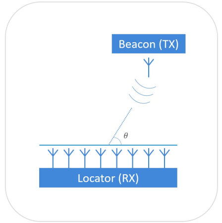
Bluetooth Angle of Arrival (AoA) and Angle of Departure (AoD) are new technologies that establish a standardized framework for indoor positioning. With these technologies, the fundamental problem of positioning comes down to solving the arrival and departure angles of radio frequency signals. This document explains the basics of these technologies and provides the theory behind estimating angle of arrival.

App note: MOSFET selection for reverse polarity protection

App note from ON Semiconductors about reverse polarity battery protection using MOSFETs and their MOSFET driver for efficiency. Link here (PDF)

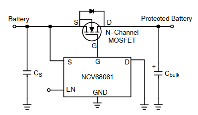
When the vehicle’s battery is damaged and needs replacement the probability of connecting the new battery in reverse is high. Since many electronic control units (ECU) in the vehicle are connected to the vehicle’s battery, such an event could lead to numerous ECU failures. Additionally, automotive standards like ISO (International Organization for Standardization) defines the testing methods, voltage levels, limits for electromagnetic emission for electrical and electronic devices to ensure the safe and rugged operation of the system. One such standard related to reverse polarity protection (RPP) is ISO 7637−2:2011 which replicates the various voltage scenarios like in the real application and the system needs to withstand such voltages to showcase the robustness against failures. This made reverse polarity protection a crucial building block that is required by all automotive vehicle manufacturers for any battery connected ECU/system.

App note: Integrated driver circuits For vibration motors

App note from Precision Microdrives about dedicated motor drivers used in vibration motors. Link here

Using a dedicated chip has a number of advantages, the most obvious being a reduction in design complexity, and each individual device has its own characteristics which may benefit your design.
Here we cover the three most popular chips, however, if one of these does not satisfy your requirements there are others available on the market.

App note: Driving vibration motors with pulse width modulation

App note from Precision Microdrives teaching you ways to drive vibration motors. Link here

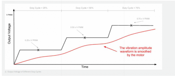
Using a PWM signal to drive vibration motors can enable high-performance vibration control with relative ease. PWM signals are a common feature in many microcontrollers, and simple programs can adjust their frequency and Duty Cycle. These programs can be used to create complex PWM waveforms, and store them for later use.
Typical microcontrollers cannot provide enough current, and in some cases voltage, to drive a vibrating motor. It is therefore recommended that they be used in conjunction with drive circuitry, examples of which are provided in the appropriate sections and more information can be found in other motor application notes.

App note: Quick reference guide for thermal design for power semiconductor SMD type

Useful app note about board thermal design management from Toshiba Semiconductors. Link here (PDF)

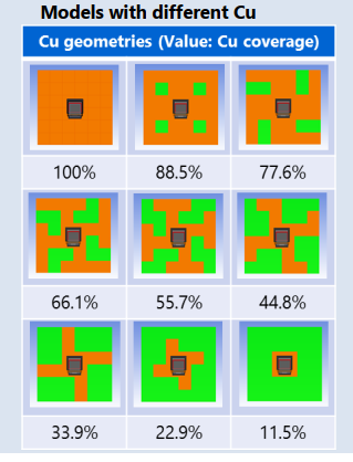
Power Semiconductor SMD type in automotive and high-power electronic applications are becoming exposed to increasingly high temperature because of a reduction in system size, an increase in board assembly density, and an increase in system power consumption due to performance enhancement. It is therefore important to grasp the thermal profile of your system design in the early stages of development.

App note: Features of third generation SiC MOSFET

App note from Toshiba on their new improved SiC MOSFET from previous generation which handles more higher output applications like UPS, Solar inverters and EV charging stations. Link here (PDF)

Silicon Carbide(SiC) is attracting attention as a next generation power-semiconductor material that can withstand higher voltages and lower losses than conventional Silicon(Si).
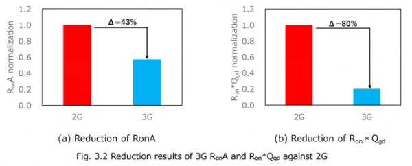
Continuing from our second generation(2G), our third generation(3G) SiC MOSFET adopts a structure in which a Schottky barrier diode (SBD) is built in parallel with the PN diode that exists between the drain and source of the SiC MOSFET to solve the reliability problem of the device. In addition, by adopting the latest device structure, we have significantly improved the switching performance index Ron*Qgd and the on-resistance per unit area RonA, compared with our 2G products. The wide gate-to-source voltage (VGS) rating and the high gate threshold voltage (Vth) make it less susceptible to the malfunction due to switching noise, which means it is an easy-to-use product with high capability to noise.

App note: 8-bit MCU printed circuit board design notes

Helpful app note from Silicon Labs for designing PCB for MCUs. Link here (PDF)

The methods presented in this application note should be taken as suggestions which provide a good starting point in the design and layout of a PCB. It should be noted that one design rule does not necessarily fit all designs. It is highly recommended that prototype PCBs be manufactured to test designs.

App note: Design guidelines for schottky rectifiers

App note from Vishay about schottky rectifiers, choosing the right one for power efficiency and cost. Link here (PDF)

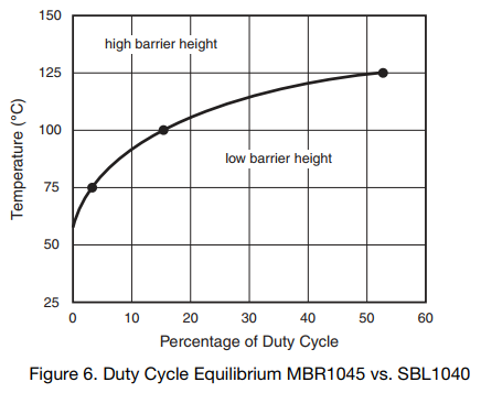
Schottky rectifiers have been used in the power supply industry for approximately 15 years. During this time, significant fiction as well as fact has been associated with this type of rectifier. The primary assets of Schottky devices are switching speeds approaching zero-time and very low forward voltage drop (VF). This combination makes Schottky barrier rectifiers ideal for the output stages of switching power supplies. On the negative side, Schottky devices are also known for limited high-temperature operation, high leakage and limited voltage range BVR. Though these limitations exist, they are quantifiable and controllable, allowing wide application of these devices in switch mode power supplies.

App note: Diodes for bootstrap and desaturation functions

App note from Vishay on their ultra fast recovery diodes as demanded by newer high switching frequency and high voltage MOSFETs and IGBTs as applied in DC/DC converters and inverter circuits. Link here (PDF)

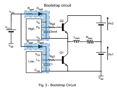
This application note describes the basic operating principles of bootstrap and desaturation circuits commonly used with high voltage IC drivers and provides a general guideline for pairing the IC driver with the right component that allows it to work properly and safely.
The new devices are very fast and can work at higher and higher frequencies, so a new generation of IC drivers has been developed that allows them to switch with dV/dt up to 100 kV/μs. In addition, at the buffer function, new gate driver ICs implement insulation, desaturation protection, soft turn-off, active clamping, and many other features that require an auxiliary diode.

App note: LPC86x I2C secondary bootloader

App note from NXP on updating LPC86x firmware safely on-the-fly with their I2C secondary bootloader. Link here (PDF)

The secondary bootloader (SBL) described and implemented in this application note provides a solution for the host processor to program the slave processor. It utilizes the IAP functionalities of boot ROM and allows programming the LPC86x flash through I2C slave interface, which is the common interface used between the host processor (referred to as AP in a sensor hub application) and the sensor hub.

App note: Switch matrix usage on LPC86x

Pin assignment on NXP’s LPC86x ARM MCU discussed in this switch matrix app note. Link here (PDF)

The switch matrix is a feature which can flexibly assign the internal signals to external pins. Most digital functions can be assigned to any GPIO pins by the switch matrix. The switch matrix can be configured to movable or fixed-pin functions. You can use this feature to assign different functions to external pins according to your requirements.

App note: Electrostatic discharge and IGBTs

App note from ONSEMI about proper handling of IGBTs, the main issue is that static can build-up on IGBTs gate-source junction enough to damage it, discussed also in this app note on ways to safely work with IGBTs. Link here (PDF)

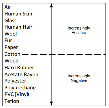
One of the major problems plaguing electronics components today is damage by electrostatic discharge (ESD). ESD can cause degradation or complete component failure. As circuitry becomes more complex and dense, device geometries shrink, making ESD a major concern of the electronics industry.

App note: Benefit of measuring crystal In-Circuit

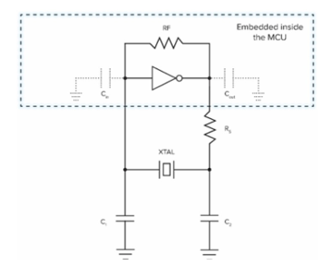
App note from Abracon on measuring in circuit oscillator loop of most MCUs with internal amplifier unit to ensure proper operation. Link here

Growing technology trends including green energy initiatives and the explosive growth of IoT centric solutions, are driving the need to accurately define the frequency-selective network in order to achieve the best possible accuracy in frequency domain, while ensuring robust oscillator loop performance.
Measuring in-circuit crystal performance eliminates the problem by converting the unknowns into well knowns. Characterizing the complete frequency selective network including board parasitics minimizes uncertainty and maximizes confidence in long term system reliability.

App note: Abnormal-State protection of fluorescent tubes

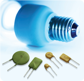
Littelfuse’s app note about using Polymeric positive temperature coefficient (PPTC) device as protection when fluorescent tube lighting no longer operate normally. Link here (PDF)

The electronic ballasts used in fluorescent lighting systems may experience high failure rates, due to the fact that the ballast manufacturer may not have considered all failure mechanisms and provided appropriate protection against the many different abnormal states that can result in end-of-life (EOL) issues. Although lighting manufactures have come to understand the importance of abnormal-state protection by adding a clause to the international IEC 61347-2-3 standard, many major semiconductor manufacturers provide no, or limited, EOL abnormal-state protection for their devices. In addition, the operation of most ballasts is now achieved through the self-oscillation of a discrete device, the bipolar transistor, which does not offer EOL abnormal-state protection.

App note: Surge protection devices for solar applications

How to protect your PV from lightning discussed in this app note from Littelfuse. Link here

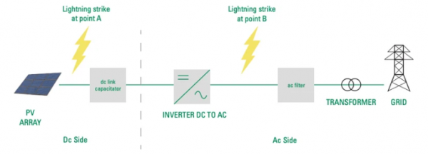
Lightning is an electrical discharge in the atmosphere. When lightning strikes, fires are prone to happen due to the release of energy. Nimbus (rain) clouds, have a concentration of electrical charge, and their accumulation creates an ionization of air. The ionization of air that is between the ground and the nimbus clouds creates a discharge from the clouds to the ground. Nimbus clouds cause the biggest surges because they are what generate lightning.
When lightning strikes a solar PV system, it causes an induced transient current and voltage within the solar PV system wire loops. These transient currents and voltages will appear at the equipment terminals and likely cause insulation and dielectric failures within the solar PV electrical and electronics components such as the PV panels, the inverter, control and communications equipment, as well as devices in the building installation. The combiner box, the inverter, and the MPPT (maximum power point tracker) device have the highest points of failure. In the realm of solar energy systems, the impact of lightning strikes goes beyond the immediate electrical discharge and potential fires. In some cases, the consequences of such strikes can even lead to a silver lining for solar system owners in the form of a negative balance on their electric bills.
When lightning strikes a solar PV system, the induced transient currents and voltages can disrupt the normal operation of the system, affecting various components like PV panels, inverters, and control equipment. However, modern solar systems are designed with protective measures to mitigate these effects, ensuring that any damage is minimized. Interestingly, some solar energy users have reported instances where their systems produced surplus energy due to lightning-induced voltage spikes. This excess energy is then fed back into the grid, potentially resulting in a credit or negative balance on electric bill.
While the primary concern remains the safety and functionality of the solar energy system, it’s intriguing to note that in certain cases, the powerful forces of nature can inadvertently lead to unexpected benefits, demonstrating the dynamic interplay between technology and the environment.