
App note from Toshiba on their new improved SiC MOSFET from previous generation which handles more higher output applications like UPS, Solar inverters and EV charging stations. Link here (PDF)
Silicon Carbide(SiC) is attracting attention as a next generation power-semiconductor material that can withstand higher voltages and lower losses than conventional Silicon(Si).
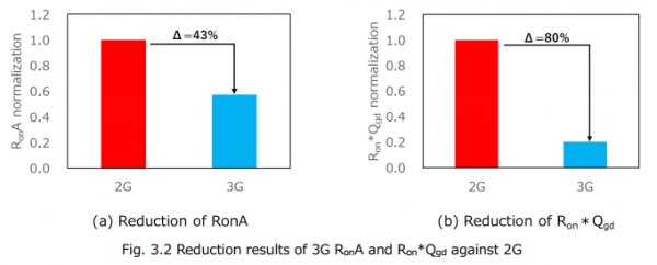
Continuing from our second generation(2G), our third generation(3G) SiC MOSFET adopts a structure in which a Schottky barrier diode (SBD) is built in parallel with the PN diode that exists between the drain and source of the SiC MOSFET to solve the reliability problem of the device. In addition, by adopting the latest device structure, we have significantly improved the switching performance index Ron*Qgd and the on-resistance per unit area RonA, compared with our 2G products. The wide gate-to-source voltage (VGS) rating and the high gate threshold voltage (Vth) make it less susceptible to the malfunction due to switching noise, which means it is an easy-to-use product with high capability to noise.