
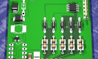

Arup is guest posting about his Nokia LCD breakout board:
I’ve designed a Nokia LCD breakout board, which was posted in this blog few days ago. That was the first version, and of course with few bugs. After numerous suggestions from the forum and the blog post, I’ve redesigned the PCB with few more fixes, and different layout.
Changes from v1 to v1α:
1. More neatly arranged components and tracks.
2. Header pin is placed in middle and mounting holes are done in 4 sides.
3. LCD is placed on the bottom layer and rest of all parts are in top layer for a clean look.
4. Equivalent SMD pads are given on every connections of DIP passives, so user can use either SMD resistor, diodes, or can choose DIP ones as per availability in his desk.
Documentation and files are available in the forum, PCBs will be available soon.
Much better – thanks!